
PRODUCTS & MATERIALS
SiC As-Cut, Lapped & Seed Wafers
SiC As-Cut, Lapped & Seed Wafers: As-cut, lapped and seed substrates are intermediate formats and are not necessarily epi-ready. Confirm cut marks, parallelism, damage removal, surface state and intended next process. For procurement, describe Diameter, thickness and tolerance, 4H/6H polytype, Si-face/C-face, off-axis angle, doping, grade, polish, defect limits. We discuss product options and inspection requirements case by case, rather than publishing unsupported stock or tolerance guarantees.
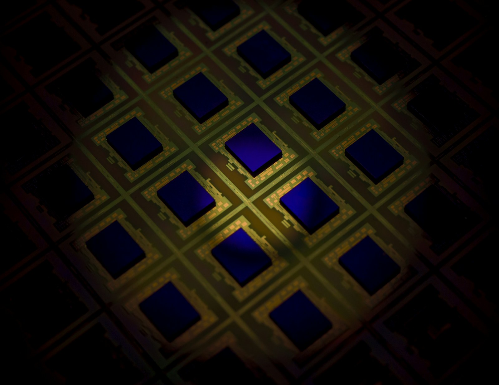
SiC As-Cut, Lapped & Seed Wafers: As-cut, lapped and seed substrates are intermediate formats and are not necessarily epi-ready. Confirm cut marks, parallelism, damage removal, surface state and intended next process. For procurement, describe Diameter, thickness and tolerance, 4H/6H polytype, Si-face/C-face, off-axis angle, doping, grade, polish, defect limits. We discuss product options and inspection requirements case by case, rather than publishing unsupported stock or tolerance guarantees.
Need a different specification?
Share your material, dimensions, quantity and technical requirements.