
PRODUCTS & MATERIALS
Compound Semiconductor Wafers
Compound Semiconductor Wafers: Compound wafers span different bandgaps, lattice constants and chemical processing considerations. Specify compound, growth method, orientation, doping, thickness and relevant inspection certificates. For procurement, describe Material and orientation, diameter, base wafer, doping/resistivity, film type and thickness, polished faces, flat/notch and inspection level. We discuss product options and inspection requirements case by case, rather than publishing unsupported stock or tolerance guarantees.
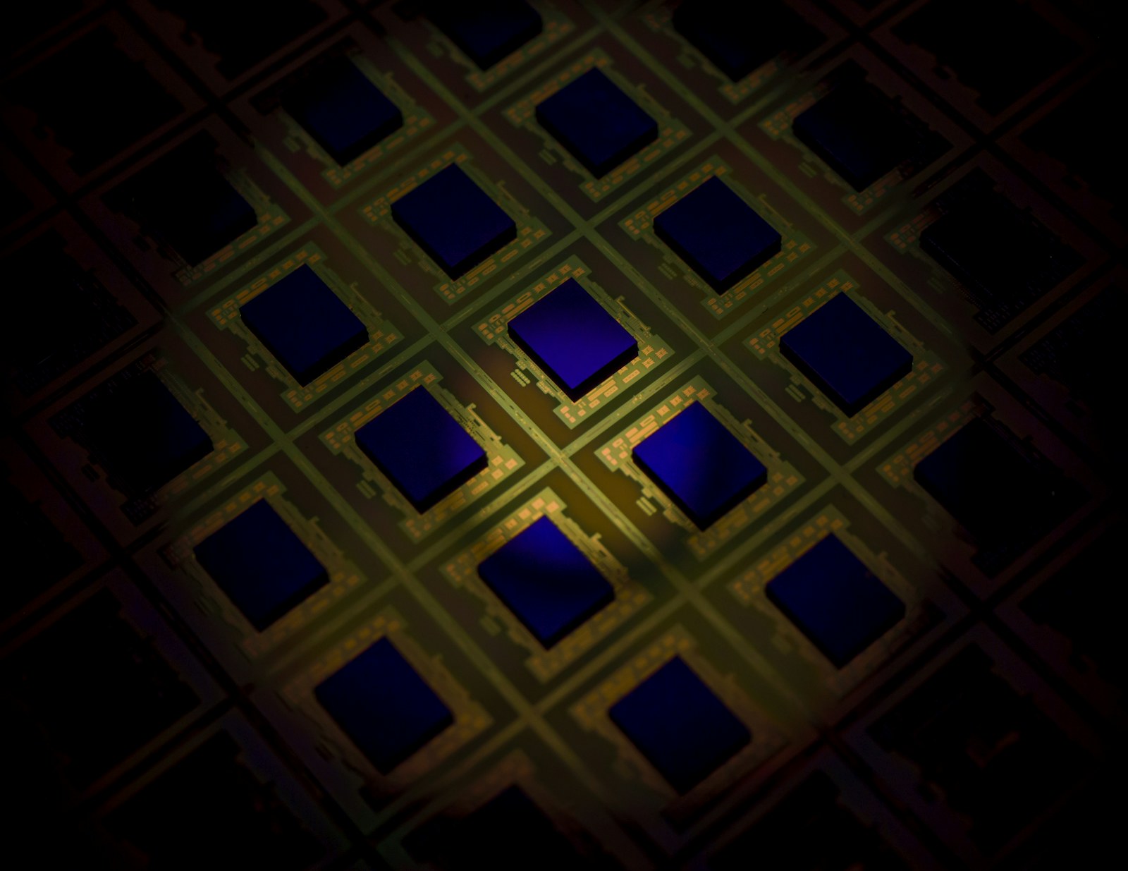
Compound Semiconductor Wafers: Compound wafers span different bandgaps, lattice constants and chemical processing considerations. Specify compound, growth method, orientation, doping, thickness and relevant inspection certificates. For procurement, describe Material and orientation, diameter, base wafer, doping/resistivity, film type and thickness, polished faces, flat/notch and inspection level. We discuss product options and inspection requirements case by case, rather than publishing unsupported stock or tolerance guarantees.
Need a different specification?
Share your material, dimensions, quantity and technical requirements.