
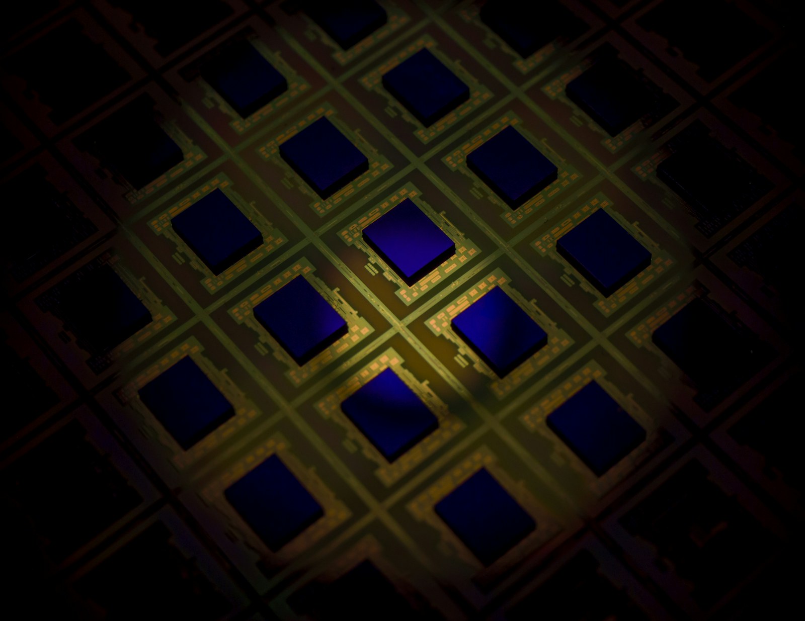
Wafer TTV, Bow and Warp
These parameters describe different aspects of wafer geometry. Know the measuring standard and your lithography or bonding tolerance before comparing quotes.
Explore wafers →TECHNICAL RESOURCES
Understand material properties, wafer quality terms and design-for-processing topics before your RFQ.
START HERE
These parameters describe different aspects of wafer geometry. Know the measuring standard and your lithography or bonding tolerance before comparing quotes.
Explore wafers →
Crystal polytype, Si/C-face orientation and doping must be specified for correct downstream compatibility, even when wafers share a nominal diameter.
Explore SiC →
Crystal orientation influences machining and epitaxy. Specify orientation, offcut, polish and surface quality for the target fabrication process.
Explore sapphire →
Borosilicate BF33 and fused silica should be treated as different materials with different thermal expansion and process limitations.
Explore quartz & glass →ARTICLES
Verified, published materials and engineering articles will appear here.
New content is under editorial review. Explore our products or send us your material specifications.
LET'S DISCUSS YOUR REQUIREMENTS
Share your target material, geometry, quantity and drawing to start a technical conversation.