
PRODUCTS & MATERIALS
Silicon & Specialty Wafers
Explore Silicon & Specialty Wafers. Wafer material, doping, film stack and surface preparation determine whether a substrate is suitable for lithography, deposition, etching, bonding or device research. Our technical catalog helps you compare possible formats and clarify the details required for a quotation: Material and orientation, diameter, base wafer, doping/resistivity, film type and thickness, polished faces, flat/notch and inspection level. Product availability, grade, dimension and test limits are confirmed only after reviewing your application.
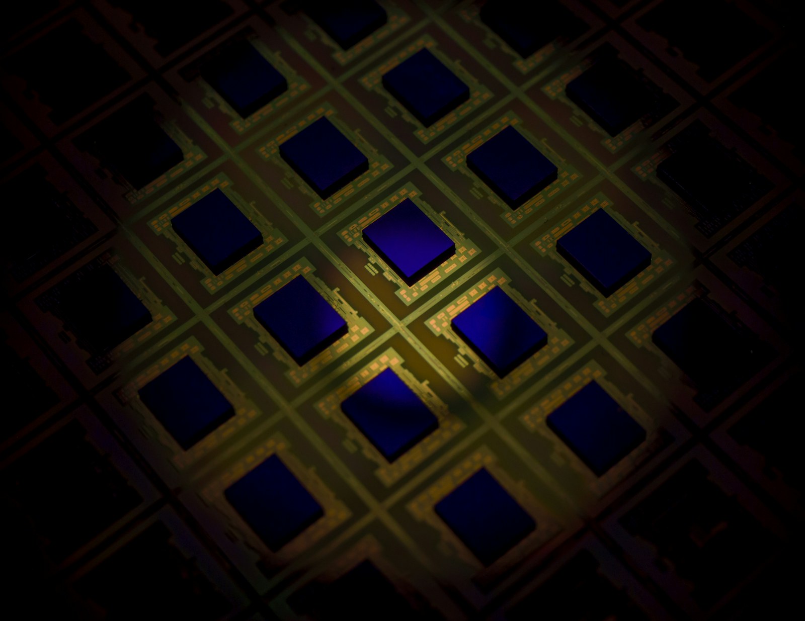
Explore Silicon & Specialty Wafers. Wafer material, doping, film stack and surface preparation determine whether a substrate is suitable for lithography, deposition, etching, bonding or device research. Our technical catalog helps you compare possible formats and clarify the details required for a quotation: Material and orientation, diameter, base wafer, doping/resistivity, film type and thickness, polished faces, flat/notch and inspection level. Product availability, grade, dimension and test limits are confirmed only after reviewing your application.
Need a different specification?
Share your material, dimensions, quantity and technical requirements.