
PRODUCTS & MATERIALS
Silicon Wafers & Substrates
Silicon Wafers & Substrates: Silicon wafer choices include crystal growth type, orientation, doping/resistivity and polish state. Define SSP/DSP, diameter, thickness, TTV and flat/notch before requesting price. For procurement, describe Material and orientation, diameter, base wafer, doping/resistivity, film type and thickness, polished faces, flat/notch and inspection level. We discuss product options and inspection requirements case by case, rather than publishing unsupported stock or tolerance guarantees.
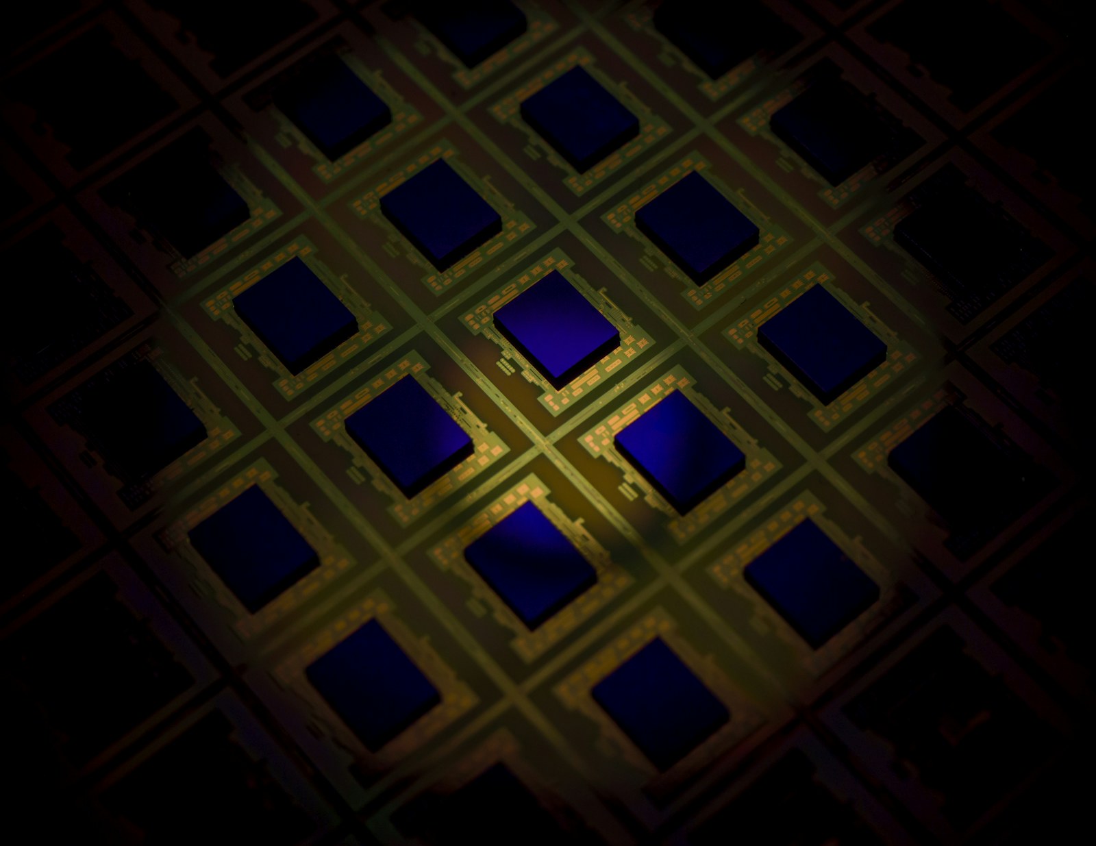
Silicon Wafers & Substrates: Silicon wafer choices include crystal growth type, orientation, doping/resistivity and polish state. Define SSP/DSP, diameter, thickness, TTV and flat/notch before requesting price. For procurement, describe Material and orientation, diameter, base wafer, doping/resistivity, film type and thickness, polished faces, flat/notch and inspection level. We discuss product options and inspection requirements case by case, rather than publishing unsupported stock or tolerance guarantees.
Need a different specification?
Share your material, dimensions, quantity and technical requirements.