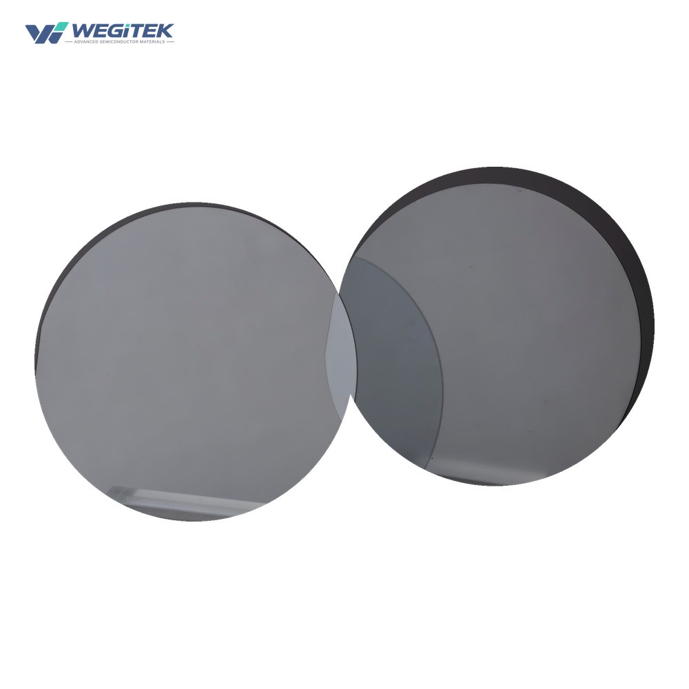
Gallium Oxide Wafer
The critical distinction for gallium oxide wafer is the combination of material grade, geometry and post-processing condition, all of which should be reflected in the specification sheet. Contact WEGITEK with your required specifications, quantity and drawings for a technical quotation.
Gallium Oxide Wafer: Material Overview
Gallium Oxide Wafer is considered for microelectronics, MEMS, integrated photonics, advanced packaging, research prototypes and equipment evaluation. Wafer material, doping, film stack and surface preparation determine whether a substrate is suitable for lithography, deposition, etching, bonding or device research. Compound wafers span different bandgaps, lattice constants and chemical processing considerations.
The critical distinction for gallium oxide wafer is the combination of material grade, geometry and post-processing condition, all of which should be reflected in the specification sheet.
Engineering and Specification Considerations
Specify compound, growth method, orientation, doping, thickness and relevant inspection certificates.
- Material and orientation
- diameter
- base wafer
- doping/resistivity
- film type and thickness
- polished faces
- flat/notch and inspection level
Quality and Inspection Priorities
Engineering acceptance should be defined before order confirmation. Depending on grade and use, the inspection review may include:
- Diameter
- thickness
- orientation
- resistivity and doping; TTV
- bow
- warp
- particle level
- edge quality and layer thickness for engineered wafers
Where possible, request the inspection method, measurement location and batch documentation alongside the numeric limit.
Applications and Selection Guidance
Potential application fields include microelectronics, MEMS, integrated photonics, advanced packaging, research prototypes and equipment evaluation. The final selection depends on thermal, electrical, optical and mechanical operating conditions. Share the process step and acceptance criteria to help the supplier evaluate feasibility.
Frequently Asked Question
What information is needed before selecting a wafer for lithography?
Confirm diameter, orientation, surface finish, thickness, bow/warp, edge geometry and any film or coating requirements. The acceptance limits should match the lithography tool and process window.
What should be included in a request for quotation?
Send the part name or drawing, material grade, diameter/size, thickness, orientation, surface finish, quantity and required tests. If you have a target delivery date or acceptance specification, include it at the outset.
Specification status: Product descriptions are reference information, not a published stock or performance guarantee. Final specifications, manufacturing options, price and delivery require written confirmation.